PCB Trace Impedance Calculator
Calculates the characteristic impedance and per-unit-length parameters
of typical printed circuit board trace geometries.
|
Select a configuration:
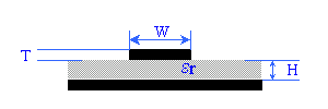
Microstrip Trace
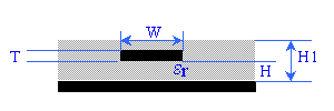
Embedded Microstrip Trace
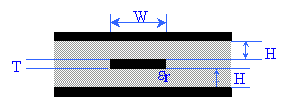
Stripline Trace
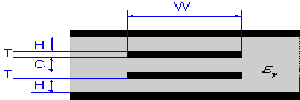
Dual Stripline Trace
|
Geometric Parameter Definitions:
| W: |
|
trace width |
| T: |
trace thickness |
| H (/H1) |
height of trace or dielectric above return plane |
| C: |
distance between the differential stripline pair |
| er: |
relative permittivity of the dielectric |
Electrical Parameter Definitions:
| Zo: |
|
characteristic impedance |
| Zc: |
effective characteristic impedance including the capacitance of distributed loads |
| Tpd: |
propagation delay |
| Lo: |
inductance per unit length |
| Co: |
capacitance per unit length |
|
Acknowledgements:
The source for formulas used in this calculator (except where otherwise noted) is the Design Guide for Electronic Packaging Utilizing High-Speed Techniques (4th Working Draft, IPC-2251, February 2001.
THESE FORMULAS ARE APPROXIMATIONS! They should not be used when a high degree of accuracy is required.
This transmission line calculator was based on a concept developed by Douglas Brooks of UltraCAD Design, Inc.
|
|