Microstrip Impedance Calculator
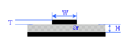
Provide values for H, T, W and the relative permittivity of the dielectric and click the button corresponding to unknown parameter Zo to calculate its value. ( 0.1< W/H < 3.0; 1 < εr < 15 )
Notes:
- The formulas used here are taken from the Design Guide for Electronic Packaging Utilizing High-Speed Techniques (4th Working Draft, IPC-2251, February 2001).
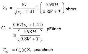
- Range of valid parameters specified in the Design Guide: 0.1< W/H < 3.0; 1 < εr < 15;
- Accuracy: For typical PCB parameters (εr = 4, H = 30 mil and T = 1.37 mil), the deviation of the calculated results from results obtained using XFX, a 2D numerical field solver from Innoveda, is listed below:
| Zo: | |
| 0.1 < W/H < 0.2 | within 5% |
| 0.2 < W/H < 1.5 | within 2% |
| 1.5 < W/H < 2.0 | within 5% |
| 2.0 < W/H < 2.7 | within 10% |
| 2.7 < W/H < 3.0 | within 15% |
| Co: | |
| 0.1 < W/H < 0.2 | within 10% |
| 0.2 < W/H < 1.2 | within 5% |
| 1.2 < W/H < 2.0 | within 10% |
| 2.0 < W/H < 3.0 | within 5% |